


Generalizing the Passive Twin-T notch filter
Begone, pesky factors of 2

The Passive Twin-T might be the most common circuit for realizing a filter that (when the right values are fitted!) delivers a frequency response that has a ‘notch’, or null, a single frequency at which there’s no output signal when a sinewave input at that frequency is applied at the input.
Oddly, there’s no specific Wikipedia entry for the Twin-T as a filter; you end up at the RC Oscillator page, which mentions a form of oscillator using the network. But we are not talking about that here, so, sorry, Wikipedia…
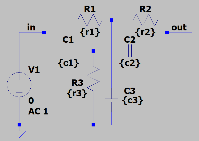
Figure 1: the general passive Twin-T
In its simplest form it’s a passive circuit containing three resistors and three capacitors (we’ll take a look at modifications with an added opamp or two another time). If you search the web for images matching the term “Twin-T filter” you will find an almost inexhaustible selection of pictures, nearly all of will share a very specific pattern of component relationships; here’s an example:
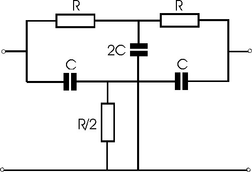
Figure 2: what nearly all the books tell you to do
The complexity of analyzing this circuit belies its apparent simplicity. As you might expect (interview question: why might you expect it?), the transfer function of the unloaded network with general component values is a third-order. The symbolic analysis tool SapWin gives you the transfer function in a few moments:

Figure 3: SapWin easily gives you the actual transfer function
Other souls have been brave enough to go further with these functions and I shall shamelessly jump to the key results that we need in order to make use of the passive form of the circuit. There are two expressions that we need: the frequency where the notch will be, and a component constraint that ensures that the notch “goes all the way down”, i.e. gives theoretically infinite rejection at that frequency.
First, the frequency of the notch is equation 1:

where CS is the capacitance of C1 and C2 in series, so CS = C1·C2/(C1+C2).
Second, the balance constraint to ensure that you do get a full notch is equation 2:

where CP is the parallel value of C1 and C2, so CP = C1+C2, and RP is the parallel value of R1 and R2, so RP = R1·R2/(R1+R2). Everyone with me so far?
Right, stare at those expressions for a few moments and tell me what’s the obvious path towards designing the network with arbitrary R and C values to have a desired frequency and also to have a proper notch.
Did you see the starting point? The expression for the notch frequency does not contain the value of R3.
That’s very useful. It suggests the following sequence:
(1) Pick R1 & R2 (and calculate RP), C1 & C2 (and calculate CS and CP), and C3, to give you the notch frequency you want from equation 1 while meeting all the other engineering constraints you might have.
What might some of those constraints be to make you depart from the ‘standard’ Figure 2 form? In my recent cases, some of these components needed to have very high voltage ratings and terminal clearances, so I couldn’t just pick any old easily-sourced precision passive components. What’s more, the values of C1, C2 and C3 were single-digit pF, meaning that parasitics on the PCB were not negligible in comparison and needed to be estimated for addition to the overall values.
Here comes the good bit. Flip the second equation upside down and multiply through; you get:
In other words, for any set of all the components except R3, there’s a calculated value of R3 that delivers the notch at your desired frequency. And we’re done!
Using a set of values that meets the ‘usual’ way shown in figure 2 meets these equations, so there’s no need to deviate from them if you can meet them exactly. What are the consequences of having to deviate from them to meet those other engineering constraints? Well, we haven’t given much thought until now about the frequency response anywhere other than at the notch and at the two other frequencies where the response is structurally obvious (interview question: what are those two frequencies and what’s the response there?). The short answer: the amplitude response on either side of the notch gets ‘soggier’.
This is a network all of whose poles (roots of the denominator of the transfer function) are real. In the standard case, the transfer function reduces to a 2nd order form because one of the poles is exactly matched by a real zero in the numerator so they cancel out, leaving two denominator poles and just the numerator notch zeroes (interview question: what form do the other two zeroes take, in this or any other 2nd order notch filter?).
The leftover denominator poles make for rather a poor filter. It gets progressively soggier as you move away from the standard form – not that this is always an issue but you do need to do your simulations just to make sure The standard form already only has a Q of 0.25, meaning that its two real roots are at -2±√3 (honestly, final interview question, derive those values knowing only that the Q is 0.25).
Darn, Figure 4 gives the game away, from an ancient Japanese website:

Figure 4: the poles and zeroes of the ‘classical’ arrangement (C1=C2=R1=R2=1)
It also gives us the transfer function for those values with numeric coefficients:

which factorizes by inspection (you can do this, right?) to:

and the cancellation, the notch and the Q=0.25 denominator should be obvious.
Is anyone reading this asking “why?” as in “why use this configuration anyway?” Well, for me, the winning value of the configuration is that the notch is achieved without any help from amplifiers running on a finite supply voltage. This means that the maximum input voltage you can apply at the notch frequency is limited only by the rating of the components. In my particular applications, a signal channel running on ±5V rails needed to be able to get rid of up to 200 Vrms of ~500 kHz while still allowing signals between DC and ~20 kHz to pass through undistorted to subsequent processing. That’s not something that regular active filters have a chance of doing.
The ‘standard’ set of component values is probably an easier bet when you want to improve the response by adding some positive feedback around the circuit (you can see this done both in Williams & Taylor and in Analog Devices’ classic tutorial note MT-225); perhaps there’s more to write about that in future, along with some thoughts about input impedance and cascading several of these networks for better rejection. Let me know if you want to know more (-8b — K