


Look, Ma, Almost No Distortion! The Class i Output Stage, Part 5 (of 4…)
Guest Author: Jon Pippard (lightly edited by me for consistency)

I was fortunate enough to meet Kendall through business and we have remained friends ever since. In 2011 was approached to build some Class-i hardware to test the concept in practical terms and here are the results.
Note: throughout this document, where THD is mentioned this is @ 1 kHz and THD(H9) measured in a 20 Hz~20 kHz bandwidth and 40 V pk-pk into 8 ohms (38 W), open-loop - unless specifically mentioned. The two spikes on the far right of the distortion plots are from the ‘scope and PC power supplies.

Figure 1: The prototype Class i circuit
Class i - a recap.
Kendall proposed the Class i moniker (i = current) as the aim of this topology is to exactly control the output device currents during the critical crossover period so that the normal class AB/B crossover gain error never occurs. This is done by an elegantly modified differential amp, which behaves as a current source at zero out and elegantly transforms to a near unity gain buffer as the demanded output current increases. Two of these amplifiers (one for each half-cycle) then control a conventional bipolar or MOSFET output stage. Thus, this is true error ’avoidance’ rather than ‘correction’.
As a consequence, the output stage never turns off, so switching distortion is also eliminated. In fact, results suggest that the standing current can be set at less than what is required for optimal class B bias, so in fact the topology is ‘somewhat green’. Distortion is a little higher under this condition, but it’s still very good.
Of course a Class i amp buys you an approximately unity voltage gain stage with power gain but no voltage gain. In fact, looking back from the load it looks approximately like a single emitter resistor and so the gain (into a load) is always less than unity. In order to build a useable amp we must add an additional building block, a voltage gain stage, and then (optionally) global feedback. If we want the lowest source impedance without global feedback then the emitter resistor values should be low.
As mentioned in Part 1, the voltage gain stage does need to have low drive impedance, and so some kind of buffer stage with voltage gain is always required. Although this need might seem trivial it has actually been quite demanding, more about this later.
The output power topology is non-critical, and MOSFET or bipolars could be used, as long as the loading on the differential input stages is kept low enough and the bandwidth permits closure of the local Class i control feedback loop.
Both mathematically and hence in simulation it can be shown the crossover discontinuity is completely removed. Thus it is possible to arrange a class B (more correctly class AB) output stage where the performance comparable to or better than pure class A, but has the dissipation of class AB. Furthermore, the bias current is held by a DC feedback loop, so that no adjustment is required and any variations due to temperature or supply voltage changes are automatically adjusted for. The pitfalls of under bias or gm doubling are completely avoided.
Class i Power Amp Design considerations
First let it be said that this design is somewhat more complex than many out there and to justify the cost and complexity the results need to be very good. The design should also be capable of working on high voltage rails so that high power applications can be considered, and the target was ±70 V rails, with the prototype currently running on ±50 V as a compromise on dissipation and available power transformers. The output is a parallel pair of transistors per side.
I had been given some prototype power amp pcbs and these were used as a way of mounting the power stage and a platform for the fuses, reservoir caps and so on. The current source power transistors were mounted on the main heatsink, whilst the controlling transistors deliberately share the ambient of the control amplifiers. My thanks to Hugh Dean at Aspen, Melbourne for these pcbs.
Kendall had produced (in the ‘90s!) some small pcbs for the Class i differential amplifier circuitry and these were used to good effect mounted directly above their respective power stages, see figure 2’s photo:
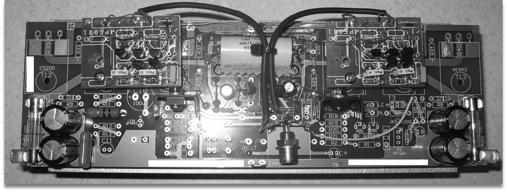
Figure 2: First prototype hardware.
Small signal stages.
The well-known 2N5401 (PNP) and 2N5551 (NPN) were selected for the small signal stages. In order to keep dissipation in these stages to a reasonable level the differential amp tail currents were initially chosen to be 5 mA. These transistors are readily obtainable in Australia, reasonably fast, have a high voltage rating and exhibit moderate Early effect.
Power stage.
The prototype power stage is a Darlington triple comprised of Toshiba 2SC2682, 2SA1142 pre drivers, 2SC4793 and 2SA1837 drivers and two pairs of 2SC5200, 2SA1943 outputs. This gives a conservative current gain of >50000, excellent power bandwidth and minimal beta droop. The maximum current is adequate for driving a 4 ohm reactive load. The topology selected is simple and known to be stable but as a precaution base stoppers of 10 ohms were used on each power device. This is a generous value but it was chosen to maximize stability and to promote current sharing of the output pair. The output pairs were also matched. Emitter resistors were 0R22 SMT types (actually 2 x 0R47 in parallel)
Protection
No protection, other than 5 A fast fuses, is used in the prototype, and the power rail is decoupled both sides of the fuse. Using the ‘free’ pcb provision is made for a triple parallel power transistor output stage if higher powers are demanded, for example to cope with reactive loads of less than 4 ohms. Conventional protection schemes could be added simply if desired.
Driving the Class I - the voltage gain stage.
Simulations of the Class i show that although the input currents are very small, typically ±20 uA, there is a very rapid change of input current around the zero cross, (as might be expected) as the Class i doublet stage does its magic. This results in ‘pre distortion’ of the input signal unless steps are taken to keep the source impedance low. In practice, 47 ohm series resistors are used within the Class i amp to protect the input transistors, and so an arbitrary max value of <<47 ohms has been placed on the drive impedance.
My original concept for the voltage gain stage employed a simple buffer based on an audio op amp chosen because it was quick, low cost and had a low DC offset. Although capable of pretty good performance, as it turned out this was not good enough. More on that later.
A little R + D
Without test equipment it is virtually impossible to guarantee what is going on, and this puts many hobbyists at an immediate disadvantage. Fortunately, software and hardware are now available at reasonable cost which allows some meaningful low frequency (up to around 10 kHz with my soundcard and PC) measurements without the considerable expense of an AP System, see ‘Test equipment’. I must confess that for this reason the HF performance of this amplifier has not been evaluated, other than to say the bandwidth of the buffer extends to at least 1 MHz.
Stability
Minor instability was cured by removing the zero in the compensation and adjusting the values up a tad. Not something that I am altogether happy with but I could not afford any stability issues during testing. Despite fears to the contrary the power stage has remained absolutely stable throughout testing despite periods of unintended abuse.
Distortion
The initial results were not promising, with distortion of 0.4% THD+N, and some signs of instability. Investigations showed that in my haste to get some working hardware, I had omitted to hook up the collectors of the driver transistors. Once the error was corrected the distortion immediately fell to around 0.06%, a much more tolerable value but still a country mile from the simulated results.
At this point I started construction of the second channel and noticed that the ‘new’ channel measured 0.02 to 0.03%. Hoping that my original stupid error had not damaged the circuit I started another witch-hunt for the variation in performance. Suffice it to say that a slightly loose speaker connection and a slightly corroded ‘crimped’ ground connection were responsible. Moral, don’t reuse old stuff unless you absolutely have to!
After putting right this inherent hardware defect both channels came in at around 0.02% to 0.03% THD. Phew...I hate amps where one channel measures differently from the other one. (Figure 3).

Figure 3: 0.03% THD from first attempt on the newly completed channel
Too much distortion
Before building this amp I modelled it comprehensively in LTspice, and even in basic form the distortion performance was very good, ~0.003% at 1 kHz and 40 W into 8 ohms.
Early on it became obvious that the simulation did not agree well with the physical amplifier in terms of the distortion performance and so investigation was necessary. It is noted in part 1 that one can deliberately produce or null even harmonics by unbalancing the circuit, for example deliberately adjusting the ratio of the emitter sense resistors to be non-unity. But the odd harmonic problem remained which was a concern as it tends to be the odds which are ‘unpleasantly’ audible.
SPICE models are not always accurate and so suspicion was cast on model transistor parameters and things such as thermal variations, layout etc., etc.
Thermal issues and a question of balance.
Right from the start the prototype exhibited quite noticeable warm up effects as the bias current stabilized. Once warmed up the bias was always stable, but the initial increase was a concern. Solid-state amplifiers should not exhibit a significant warm up period!
Unfortunately the current mirrors were not constructed in a fashion which minimizes thermal drift as there is no thermal coupling between devices on the small daughter boards. The layout actually makes this quite hard to achieve as the TO92 pairs are mounted side by side. The current mirror experiences a significant disparity between the controlling and driving transistor power dissipation of around 80:1, and so one can expect the ratio of the mirror to change and with it the set bias current. This can be minimized by using significant emitter resistor drops, as per Kendall’s original circuit and/or by elaborating the mirror. I determined that as long as the transistors were coupled thermally and the tail current reduced to a minimum this was sufficient, at least to prove a point.
But this effect goes deeper than just warm up drift. Up till now I confess I had not fully appreciated the full implications for the Class i doublet transistors. In some ways these suffer the same issues as the current mirror, one transistor is always hotter than the other (roughly 2X the dissipation at 40 V p-p out) and thus the symmetry is compromised. But what I had not realized is that the match of these transistors is absolutely critical to the distortion performance. It becomes obvious with hindsight, because any mismatch in the ‘handover’ from one device to the other is translated directly into a wobble in the crossover region. It might be said that this is the ‘Achilles heel’ of this circuit because these two devices must accurately track each other if the performance is not to suffer. The crossover issues are moved back to a lower power stage. But with matched dual transistors available the problem can be resolved. In fact, these are not strictly necessary.
By changing the IS device parameter (actually the thermal leakage) in Spice for the 2N5551 and 2N5401 models it is possible to simulate the imbalance and immediately the distortion jumps to 0.03% or thereabouts for 50% variation in IS. Unfortunately this is the natural tendency when running as the input side Class i transistors have about 50% lower dissipation than the output side, and this creates an imbalance across the differential Class i pair. Hence at power up the distortion might be <0.001% but it quickly rises as unequal device heating occurs.
This increase in the differential dissipation is proportional to the output signal, so for zero power out in theory at least the transistors share perfectly. But as the output amplitude demanded increases so the thermal imbalance increases. This is because the currents in the transistors have differing form factors which are also subject to varying amplitudes. (Figure 4):

Figure 4: ‘Class i’ doublet dissipations at 40Vp-p
How critical is this match? The nominal difference in VBE of silicon transistors of a similar type and batch is reportedly no worse than 20 mV (Ref 1) or about 4%. My experience with the Fairchild transistors I have (all from the same tape) is that it is typically 4 mV to 10 mV. As the tempco is -2.2 mV/K, that means that a junction temperature difference of 5 °C might be a worse culprit than the absolute match between the devices.
If we assume a typical TO92 transistor is rated at 0.3 W dissipation which makes for a 150 °C junction temp in a 25 °C ambient, then the junction to ambient thermal resistance will be 125/0.3 °C/W, or 416 °C/W. Thus if the first transistor dissipates 0.014 W (SPICE at 40 V p-p) the junction temp rise is 0.014*416 = 5.8 °C and the second 0.034 W (also from SPICE) we have 0.034*416 = 14.1 °C, so we have a 8.3 °C difference or approx 18 mV worth of offset.

Figure 5: Devices thermally coupled, 5 mA tail current
By using aerosol ‘freezer’ spray one can adjust the match of these transistors at will in circuit and sure enough, at one point, applying freezer to the higher dissipation transistor only of the Class i doublet (the one which tracks the output voltage) and allowing it to warm up gently produces a further reduction in distortion to >0.001% as the VBEs match. An (albeit fleeting) view of perfection!
Thermal coupling is thus mandatory. Once coupled, one can spray the pair with impunity and hardly any shift in THD is noticeable. Of course the ‘proper’ fix is the use of a matched pair for the Class i and ‘mirror’ transistors and fortunately these are available for the 2N5401 and 2N5551, but they are not mechanically compatible with my ‘low cost’ assembly.
This done, things are better with consistent values typically of 0.01~0.02%. (Figure 5) Note that the remaining distortion is almost all odd harmonic. The circuit remains untrimmed for 2H. If we then reduce the tail current to 2.5 mA the thermal imbalance is further reduced and the distortion becomes ~0.005% and we are a bit closer to perfection. (Figure 6):

Figure 6: Tail current 2.5 mA and thermal coupling. 42 W 8 ohms.
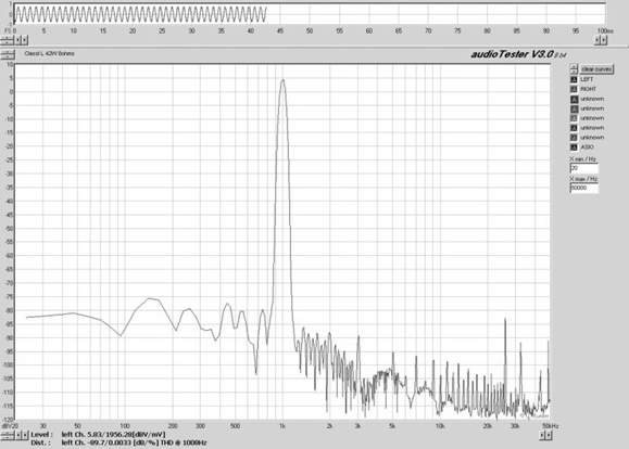
Figure 7: As figure 6, but with ‘nulling’ by application of freezer spray. Note level +5 dB to maximize dynamic range.
In figure 7 I managed to partially snapshot the effect, but just missed the null which was <0.001%, so the recorded distortion is 0.0033%. Note the reduction in odd harmonics. The level is +5 dB which translates to ~120 W into 8 ohms.
Global feedback
So far all the results presented are all taken of the Class i buffer, open loop. By applying 20 dB (10x) of global feedback we should be able to reduce 0.003% to 0.0003%. This is easy to say, but of course it depends on the ability to build a 50 dB gain block (20 dB for the FB loop gain and 30 dB of closed loop gain) with sub 0.0003% distortion, and this is not easy. Adding global feedback around the existing blocks did nothing for the distortion which remained roughly constant. It does modify the harmonic content and sound quality, not for the better.
Here is an interesting paradox; feedback works because we assume perfect ‘model’ amplifiers (specifically infinite input impedance, zero output impedance, infinite gain and hence zero distortion) and we are taught that in the case of an imperfect amplifier a loop gain of 20 dB makes a 10x distortion improvement in the output. In most traditional power amps the output stage distortion is high, whilst the input stage distortion can be made vanishing low in comparison. Put the two together and assuming 20 dB of feedback at 1 kHz, our 0.1% output stage distortion becomes 0.01%. But not so here because the output stage distortion is already around 0.003%. Applying 20 dB of negative feedback should make the output distortion 0.0003%, but the rest of the amplifier is incapable of such a low value, so slowly any hope of improved performance ‘bottoms out’. Unfortunately this is exactly what happens here, my original op-amp based buffer is simply not good enough, 20 dB of feedback has no effect at all on the distortion.
A very low distortion driver
It’s time to read up again on Doug Self and his low distortion designs (ref 3). Using the ‘load invariant’ amp as a basis of a class A driver should produce distortion numbers which are in the sound card noise floor, and so this was the route I took. I already had the ‘official’ pcbs built from some work I did in the 1990’s.

Figure 8: ‘Self style’ low distortion class A buffer with modifications due to author.
Further Improvements
Various other modifications, implications and additions can be exploited to reduce the distortion even further, the most obvious is running closed loop. With the buffer shown it is possible to put some 30~40 dB of loop gain around the buffer which should result in distortion well below my measurement capability. I intend to leave these for another time.
A note on test equipment
Initial results using a Creative Labs X-Fi card were acceptable, but not really good enough. The X-Fi card can resolve about 0.006%. I wanted to get as close to the raw performance of the AP Sys 1 I used to have access to as possible. Trawling eBay resulted in a semi pro EMU 0404 PCI card for just $41 which supports ASIO, 192 kHz sample rates and 32-bit floating point arithmetic. Software is Uli Muller’s excellent Audiotester V3.0. See www.audiotester.de.

Figure 9: EMU 0404 PCI Noise floor, 8192 samples 5x average
Using this setup it is possible to measure down to around 0.0005% without resorting to any tricks to increase the distortion components, for example by adjusting the amplifier noise gain. The downside is that really the HF distortion measuring performance is rather limited. I believe the 10 kHz numbers but above that I am not so sure. PC’s are noisy things and the two spikes to the right of the graph are the PC power supply and monitor
Finally you need a ‘scope just to check for funnies, instability, clipping etc, otherwise it can all get very misleading, a DVM and ideally a signal or pulse generator to check the square wave response.
Summary
Class i is, to my knowledge, a new technique of considerable engineering elegance. It works both in theory and practice, within the bounds of my constructional ability, test equipment, finances and time constraints.
Some defects remain and the primary one must be the matching and thermal management of the Class i doublet transistors. This may put a limit on the ultimate performance, but it should be possible to improve on what I have here, either by hand matching or ideally by employing DMMT5401/ DMMT5551 matched pairs.
Class i taken to its logical conclusion should enable a virtually distortionless amplifier, with very wide bandwidth and zero global feedback to be built. There is local feedback of course, but it’s tightly confined in local loops of very high bandwidth. Furthermore, any distortion remains substantially low right across the accepted audio band. If one then wishes to ignore current fashion and use modest global feedback the results should be exemplary.
Jon Pippard, Melbourne, Australia
References
1) Operational Amplifiers Burr-Brown McGraw Hill 1971 Tobey, Graeme, Huelsman
2) Audio Power Amplifier Design Handbook 2nd edition Newnes 2000 Douglas Self MA, MSc
3) Self on Audio 1st edition Newnes 2000 Douglas Self MA, MSc