


Yet More On Decoupling, Part 1: The Regulator’s Interaction with capacitors
time to give these articles a new audience

This revised 2008 article was published on EDN in 2013. I made no attempt either then or now to bring some elements up to date. For instance, I refer to Linear Technology’s '“SwitcherCAD”, which at the time was the wrapper for the LTspice simulation engine. That simulator has gone from strength to strength, still solidly supported by LT’s new home, Analog Devices, but you can see how useful this was even 17 years ago (that makes me feel old).
All my graphics for the articles were created and saved as metafiles so it’s taking me a little while to turn those into something that Substack can cope with!
In a 2007 article, “Know the sometimes-surprising interactions in modelling a capacitor-bypass network” (https://www.planetanalog.com/know-the-sometimes-surprising-interactions-in-modelling-a-capacitor-bypass-network, abbreviated to “Know the...” when referred to here), Tamara Schmitz of Intersil and I provided some simulation background behind the interaction between multiple decoupling capacitors used in parallel. The series inductances inherent in the capacitors cause several resonant peaks and dips in the impedance response, sometimes at frequencies that might be critical for circuit operation. We advised that, if you intend to use decoupling capacitors of different values in parallel (there’s almost always more than one capacitor attached to the power rail), you’d better be sure that the location of the resonant peak won’t cause trouble in your circuit. But we didn’t say what kind of trouble that might be.
So this series of articles is an attempt to quantify what’s happening on the supply line of a representative analog circuit with regulated supply rails and decoupling capacitors. We’ll do this entirely in simulation – mainly to show that this is both possible and revealing – and the path to interesting results will prove a somewhat bumpy one. Over the course of the six articles we will:
· look at the overall supply impedance seen by a component when we include the decoupling caps, the voltage regulator and the board traces providing the component’s power. In passing, we’ll discover just how supply voltage affects the value of some ceramic capacitors;
· see how such an impedance responds with a characteristic voltage transient when you ‘ping’ it with a current change such as an IC might demand from the power rail. Choice of capacitor dielectric turns out to have a significant effect;
· see how these supply variations punch through to the output of an op-amp running on these supplies;
· discover that many op-amp simulation models, used for this purpose, are so inaccurate that they can produce seriously misleading and even physically impossible results;
· run a signal through the attached op-amp, drive a load, and see how the actual load current (rather than part 2’s test current ‘ping’) interacts with the modelled supply, and how this affects the amplifier output;
· see that simulations provide an objective approach to selecting decoupling capacitors in order to alleviate a previously poorly documented effect on the precision of op-amp circuits. And discover another way in which many op-amp simulation models are so inaccurate they are useless for this work!
Paralleled decoupling capacitors – the story so far
If you didn’t catch them first time round, why not first review the article linked to above. The graphs in that article show the dramatic impedance excursions possible with paralleled decoupling capacitors of different values. A valid criticism of these plots is that they just refer to the capacitance that the device sees. They don’t include the impedance actually already present on the power supply rail, determined by the voltage regulator (which usually also has its own output capacitor), and the tracks or power planes that connect them all up. They don’t reflect any loss mechanisms that might lessen the severity of these effects. First step, therefore, is to rectify these omissions. Now, instead of just looking at just the theoretical impedance of the decoupling capacitors themselves, we’ll connect up a ‘real’ regulator IC to ‘real’ capacitors and connect all of this to a ‘real’ amplifier which is handling a ‘real’ signal. All in our virtual world, of course.
For all the simulation work in these articles I’ve used SwitcherCAD 3, which uses their LTspice simulation engine, and is available free from the Linear Technology website (http://www.linear.com/designtools/software/switchercad.jsp). If anyone is interested in experimenting further with the material presented here, I’ll be uploading the test files to the LTspice Users Group (http://tech.groups.yahoo.com/group/LTspice/), so that you can reproduce this work and adapt the fixtures to your own needs. I had loaded SwitcherCAD up as part of another project to fearlessly evaluate, on your behalf, some of the free software out there for circuit simulation, and for filter design (something close to my heart). The LTspice engine seems to be admirably robust, accurate and speedy, and SwitcherCAD comes with a large library of Linear Technology op-amps, regulators and other devices, which I used here as typical of the parts that would be used on a quality, precision analog design.
After some browsing through the SwitcherCad library I chose the LT1761-5 and LT1964-5 as the +5V and -5V regulators for the dual supplies on this virtual project, on the assumption that it will be handling bipolar analog signals. These are low-dropout regulators (LDOs); this type of regulator is commonly used for local regulation of power on analog subsystems.
The regulator’s output capacitor
The LT data sheets indicates that output capacitors with low ESR value can be used with these parts, which is not always the case with low dropout regulators. The regulators were each operated with a 2.2uF output capacitor, and the common choices for that part would be a ceramic or a tantalum device. On cost grounds, my initial choice was a ceramic component, and additional help on capacitor parameters was taken from the program SpiCap3 which can be downloaded for free from AVX’s website (http://www.avx.com/SpiApps/default.asp).
SpiCap3 provides an LCR capacitor model for any AVX ceramic capacitor, given operating conditions such as temperature and voltage, which change the capacitance of high value ceramic caps in a big way. The program was used to check parasitic inductance and ESR, and it provided some eye-opening insight into voltage dependency. I initially chose Y5V dielectric for the 2.2uF ceramic alternative, on the basis that temperature and voltage performance weren’t likely to be significant, while small size and low cost was. But when you dial in the voltage across the capacitor you find that at 31% of rated voltage – 5V used on a 16V part – the capacitance is down to one quarter of the rated value! In other words, my chosen Y5V 2.2uF part was only a 0.55uF capacitor. Note that while 2.2uF is above the specified minimum output capacitor value for these regulators, 0.55uF is below it, so you’d be violating LT’s guidelines without realizing it. Note to AVX: why not make setting working voltage easier to do in the program? Each time you change the rated voltage you have to reset the percent of rated voltage slider, why not have the user enter an operating voltage and get the program to scale it?
As designers, we all know that voltage dependency in high-k ceramics is an issue. But when the information is right there in front of you, it becomes much more real, and a huge red flag for all users of high value ceramic capacitors. The final ceramic choice was a 16V 1206 part with ESR of 8 milliohms, and an X5R dielectric to ensure that the actual value under 5V bias is 2.1uF, pretty close to nominal. Another note to AVX: how about having the program tell you the part number of the component you just selected?
Getting on track
Printed board construction varies greatly, and this affects the impedance of the power supply connections at low and high frequencies. I couldn’t find comprehensive models for typical printed circuit traces and started out with standard microstrip models, using the formulas in http://emclab.mst.edu/pcbtlc2/microstrip.html to estimate inductance and capacitance (the latter is entirely negligible here), and straightforward physics to get the resistance.. Nevertheless, a referee of an early draft of this paper felt sure that some acknowledgement of skin depth loss in the PCB traces would be needed, to produce simulations which better reflected physical reality. Accordingly, I adapted some published work on the losses that skin effect introduces into high speed cables.
The specific dimension I’ve taken for my copper power trace is: length 50mm (one-tenth of a wavelength long at 600MHz, I’m only planning on analyzing up to 100MHz), width 1.27mm, thickness 35um (1oz copper, though sometimes inner layers are thinner than this), on a 4-layer board with the ground plane on an adjacent layer.
only ground this morning
Whatever you like to call it – ground, GND, 0V, Vdd, common – this connection causes just as much trouble in simulation as it does in the real world. Ironically, it’s because the ground net in SPICE is perfect, ubiquitous and available anywhere in your circuit at a mouse-click that it yields physically unrealistic results. The makers’ device models also have a rather unhealthy relationship with GND, as we’ll see. As far as the project layout goes, I’ve referred all the inductance impeding the flow of supply current to the supply connections – it’s the total voltage variation at the amplifier under test that I’ll be interested in, and won’t be asking tough questions about ground voltage variation across my ‘circuit board’.
Before we actually fit an amplifier, we’ll just look at the decoupling. We’ll consider a single capacitor per rail (this is in addition to the output capacitor of the regulator), and step its value from 22nF to 470nF, a pretty common spread for single decoupling capacitors. The SpiCap3 program gave ESR values for each cap choice once I’d decided size and voltage (X7R dielectric used in all cases), but the spread was not that dramatic so an average value of 33milliohms was used. Another parameter I’ve made constant is the parasitic inductance of the capacitor. This is determined by capacitor body size and mounting details, as discussed in “Know the...”. As the capacitor value gets larger, the chosen size of the capacitor rises from 0402 to 0603; for simplicity I have included a constant 0.7nH for the parasitic inductance and have ignored the ~0.2nH difference you’d get between the two case sizes. This doesn’t have significant effect on the results here.
All together now...
Figure 1.1 shows the test circuit so far: regulators with their ceramic output capacitors, with 20mA of (constant) load current taken out of them; power supply traces with some skin effect modelling, and a capacitor which we’ll be using as a decoupling device for some subsequent electronics. Figure 1.2 is a busy graph showing various impedances calculated as the AC voltage response on the supply rail divided by the value of the test current source, plotted in dB referred to 1 Ohm. Because the test current has a value of 1, just plotting the voltage also gives the impedance. Don’t worry, this is a linear, level-independent analysis, it doesn’t mean I’m using a test current of 1 Amp!
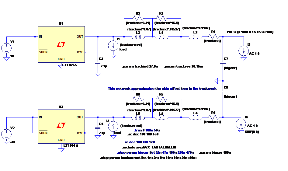
Figure 1.1: basic supply impedance test circuit.

Figure 1.2: basic supply impedance test results.
There’s a lot going on here. The red traces show the change in impedance of the decoupling capacitor as it is swept; no surprises there. As the value falls, the mow frequency impedance rises, as does the notch frequency where it’s resonating with its self-inductance. At very high frequencies the impedance is rising and isn’t dependent on capacitor value.
The blue trace, shown just for the negative rail, is the apparent impedance of everything else connected to the decoupling capacitor. At very low frequencies the impedance is low, as you’d expect for a regulator. As the frequency increases, the impedance rises – why, we’ll come to in a moment. Then above about 10kHz it starts to fall again, and it reaches a minimum just below 1MHz. This is the frequency at which the regulator’s output capacitor resonates with the layout inductance. After that the impedance rises – we are just seeing the impedance of the power trace.
The green traces show the combined effect, shown this time for the +ve rail, primarily to illustrate that the ‘bump at 10kHz is there as well, and it has a pretty similar shape. As expected from “Know the...” there’s now an impedance peak in between the notches; its height (i.e. the ‘Q’ of the resonance) and frequency increase as the decoupling capacitor value is reduced. Shortly we’ll start to look at what happens when some current is demanded from this strange, peaky impedance.
But what about the impedance bump around 10kHz – what component is causing this resonance – looks like it must be a very large inductor? Well, it’s the regulator itself, and here’s why. An LDO’s output stage is basically a buffer amplifier with high-ish output impedance and feedback around it to bring that down. The internal amplifier has only moderate bandwidth and approximates an integrator, as indeed the vast majority of op-amps do (hold that thought for the next part). This helps the regulator to be stable with a variety of reactive loads. So the effectiveness of the feedback in reducing the output impedance lessens at higher frequencies, and so the output impedance rises with increasing frequency. The regulator thus acquires an inductive output impedance.
Feeling a little ‘peaky’
The ‘bump’ at 10kHz is the result of this inductive output impedance resonating with the 2.2uF output capacitor. And it changes with the load current; figure 1.3 shows a load current sweep from 1mA to 50mA. At lower currents the height of the impedance peak can rise dramatically. Some LDO regulator data sheets do tell you this in the graphical small print at the back, but often don’t dwell on the consequences. We can also see that the two regulators don’t behave in the same way as current is changed. Green trace is the composite for the decoupled +ve rail; both rails look the same at high frequencies. Blue trace is the –ve regulator and traces at low frequencies, and represents either regulator at higher frequencies. In the figures, the decoupling capacitor is held at 100nF (red trace).
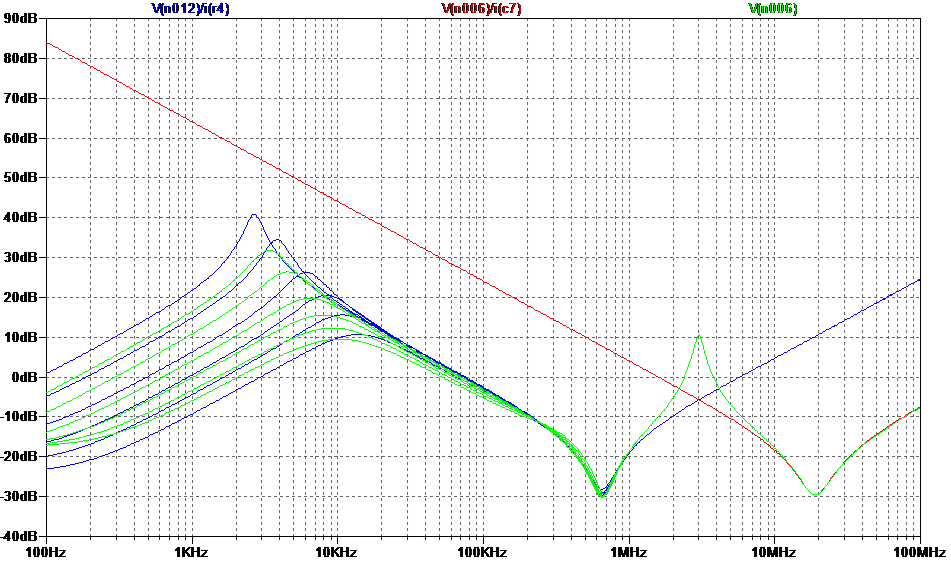
Figure 1.3: variation of the regulator’s effective inductance with load current.
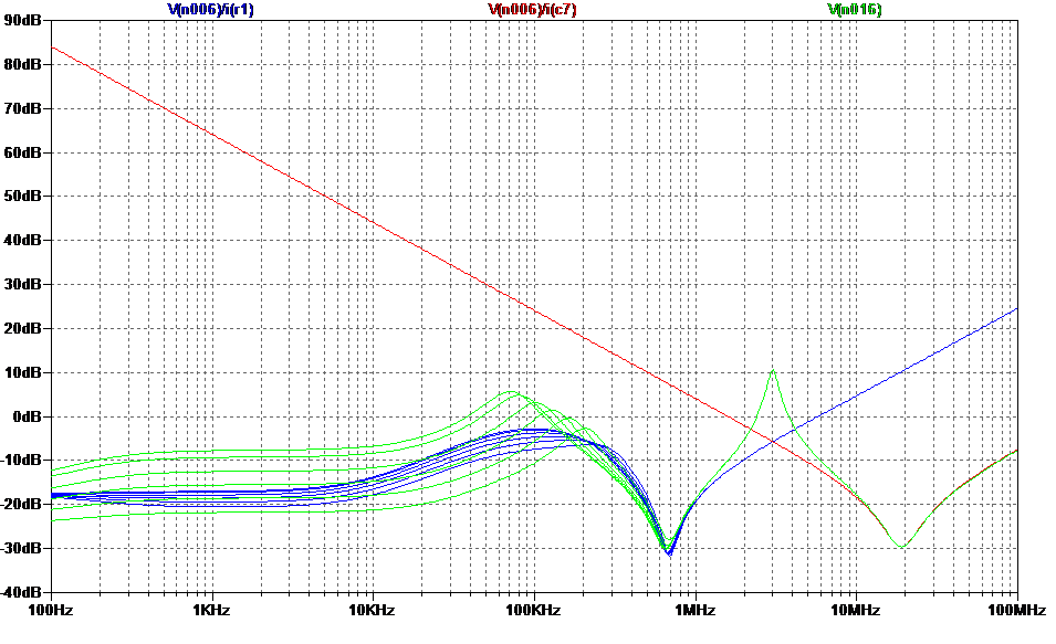
Figure 1.4: as figure 1.3 but with ‘noise bypass’ caps fitted.
The makers of these particular regulators have thoughtfully provided an extra pin, which can be connected back to the output with a capacitor (the noise bypass capacitor confusingly also called a ‘bypass’ capacitor). This reduces the high frequency gain, with the main intention of reducing the output noise of the regulator. Does it also have an effect on the output impedance? It sure does, figure 1.4 shows how the peaks can be managed by attaching a suitable capacitor (not the same for each regulator; I used 2200pF on the +ve regulator and 150pF on the –ve regulator). The tracking and matching is not perfect but it looks to me like a worthwhile improvement, because not all circuits attached to these supplies can be assumed to have perfect power supply rejection performance. To be continued...
Takeaways from this part:
· If you are using Y5V capacitors with DC bias across them – as you always do in a supply decoupling application – carefully calculate the effective capacitance value. You could be ‘out’ by enough to seriously impair circuit performance and reliability.
· LDOs have an effective output inductance; it varies with output current (goes higher as the current falls) and causes an output impedance peak with the output capacitor. Use an LDO with a “noise bypass” capacitor connection to flatten out the impedance.
2013 Postscript
Regular readers of my columns will know that I’m as appreciative of Linear technology’s simulation platform today as I was five years back. This series was the beginning of my love affair with the best free electronic engineering tool on the web. The name has changed, and the product has become faster and more stable. But even five years ago it did a great job on the simulations I needed. I must admit that I do a lot more simulation and a lot less construction these days, compared to say fifteen years ago. Some old-school engineers have wondered whether that’s too much like going over to the dark side. Tailors say “measure twice, cut once”. For me, it’s “simulate thousands of times, build once”. These days I would not dream of building something with matter before exhaustively probing it with mind.
The main comments I received about this first part centered around the transmission line modeling approximations that I had used for printed circuit board traces. Cheap circuit board materials can introduce rather more loss than represented by these simple models. When pressed, my correspondents admitted that they probably relied a little too much on “getting away with it”. As better materials and components are chosen to suit today’s higher speed digital signals, much of this loss goes away. As designs get ever more compact and lower in cost, physically large lossy chemical capacitors are frequently replaced with small low-loss ceramics. In the last five years I’ve encountered several cases, and heard of more, where removing chemical caps had some unexpected consequences. The moral: always have one component per rail on your board whose main job is to introduce loss on each power rail. A small, low value resistor in series with one of the high-value ceramics will do the job. A supply without designed-in losses is like a car suspension without shock absorbers – you could get a rough ride!
Every generation of audio equipment designers rediscovers that you can change how audio systems sound by changing component types and values. Several audio friends of mine reported interesting results from ‘tuning’ the resonance between the LDO and the main output capacitor, as I suggested here. Douglas Self’s books, particularly his recent one on audio filter design, have made a big contribution to the canon since I first wrote these articles, showing that component choices can have surprisingly large measurable effects in audio equipment.