


Yet More On Decoupling, Part 2: ring the changes, change the rings

Previously on “Yet more...” we built up a pair of regulators with output capacitors, and connected them to some decoupling caps with a short length of copper trace. We looked at the impedance at these decoupling caps, and saw some peaks. What happens when we start taking some current from these imperfect supplies?
Figures 2.1 and 2.2 show what happens in the time domain when we take a squarewave current switching between 0 and +10 mA at 100 kHz from the positive regulator, and one switching between -10 mA and 0 on the negative regulator. The rationale is that later on, we’ll either be taking current from the +ve rail, or dumping it into the –ve rail. Remember that the regulators have a static load of 20 mA as well, so we are not taking regulator current down to zero. The swept parameter is once again the value of the local decoupling capacitor, 22 nF (top trace, blue) to 470 nF (bottom trace, pink), and the traces are offset from the top down by 10 mV each time.

Figure 2.1: pinging the positive rail with 100 kHz 0 to +10 mA square wave, 5 mV/div, traces spread by 10 mV.
As expected, the smallest capacitor shows the highest amplitude of additional ringing, occurring at the highest frequency. As the capacitor value goes up, the magnitude of the ringing falls. Constant in all this is the effective impedance at the 100 kHz fundamental, which seems to be about 0.7 ohms for either supply. Note that these voltages are in phase. The frequent assumption about the supply variations being symmetrical around ground is not true in this case; indeed, hardly ever true.

Figure 2.2: pinging the negative rail with 100 kHz 0-10 mA square wave, 5 mV/div, traces spread by 10 mV.
The high frequency ringing looks unsightly and may well impact our circuits – what could we do about that? We need some damping somewhere, perhaps by adding some series resistance to one of the capacitors. This will help to dissipate stored energy in the resonant circuits more rapidly, reducing the ‘Q’. Now, with other regulator designs we might have been forced to have this extra series resistance, because some LDO designs are not stable when the main output capacitor has too low an ESR. Often in those designs a tantalum capacitor is used, so let’s pick one.
AVX used to have (2024 note: I haven’t yet found where it is now) a useful utility on their download page, SpiTanII, which assisted with the selection of tantalum capacitors, and the associated SPICE library contains models which accurately portray the frequency-dependent loss of that type of cap. This should lead to much more accurate simulation than just guessing a resistive ESR value. A 2.2 uF 1206-sized part (TPSA225K016R1800, same footprint as the ceramic previously deployed, and with 16 V working voltage) was chosen; it has a rated maximum ESR of 1.8 ohms at 100 kHz, which is about as good as it gets for a small tantalum. Important tip: fit this capacitor the right way round in your simulations. In the simulation world as well as in the real world, the tantalum capacitor doesn’t work properly under reverse polarity!

Figure 2.3: same as fig 2.1 but using a 2.2 uF tantalum output cap on the +ve regulator.
What a difference; a lot less high frequency rubbish (especially on the –ve rail which is not shown). The impedance curves show why; with the tantalum capacitor, the +ve regulator particularly is still showing some peaking just below 1 MHz. Still, looks like an improvement, but we will keep testing this choice in the work to come, to see what consequences the ringing has.

Figure 2.4: impedance plots of the supply rails with tantalum capacitors. Contrast with figure 1.2 in part 1.
Can you hear me?
Most of this work is concerned with effects in the MHz region, but in passing, let’s look at what happens with lower frequency stimulation of the rails. This may be interesting for people working on audio applications.
Figure 2.5 shows the rail impedances as we step up the regulator output capacitor from our current 2.2 uF up to a whopping 2200 uF (ESR was set at 0.1 ohm for all of them, as might come from a physically large aluminium electrolytic used in audio circuits). The decoupling capacitor was fixed at 100 nF; none of the high frequency effects pointed out earlier are relevant at this timescale. As the capacitance value increases, the audio band impedance becomes flatter, then finally rather less flat as the very largest capacitor does a better job than the regulator does. Figure 2.6 shows the voltage response of the +ve rail to a test current of 0-10 mA at 333 Hz.

Figure 2.5: rail impedance as we increase the regulator output cap from 2.2 uF up to 2200 uF, decade steps. This is with the noise bypass caps.
As the output capacitor increases, it provides progressively more ‘support’ for the regulator. Going only on the traces in figure 2.6, it looks like a 220 uF capacitor would do a good job of delivering an ‘uncolored’, frequency-independent output impedance in the audio band. The square-wave response for the 2200 uF is actually less accurate, though judgements like these will depend on the actual test frequency and there’s no one “right answer”.

Figure 2.6: voltage on the rails when 0-10 mA squarewave at 333 Hz is applied. 2.2 uF top, 2200 uF bottom.
Remember that we suppressed some impedance peaking at 10 kHz in part 1 by adding the noise bypass capacitors. What happens if we lift these off and run this test again?: The resulting rail impedance is shown in figure 2.7; the location of the peak falls as the output capacitor is increased, but even with an enormous 2200 uF capacitor it’s still well into the audible band. The consequences of this peak are clear in the current transient test. Perhaps it’s not surprising that advocates of ultimate audio quality insist that capacitor selection can have an effect on a system’s sonic performance even where you’d think it couldn’t, like on the output of a regulator. Fit those noise bypass caps!

Figure 2.7: as figure 2.5 but with the noise bypass capacitors removed. Note the resonant peak in the audio band.
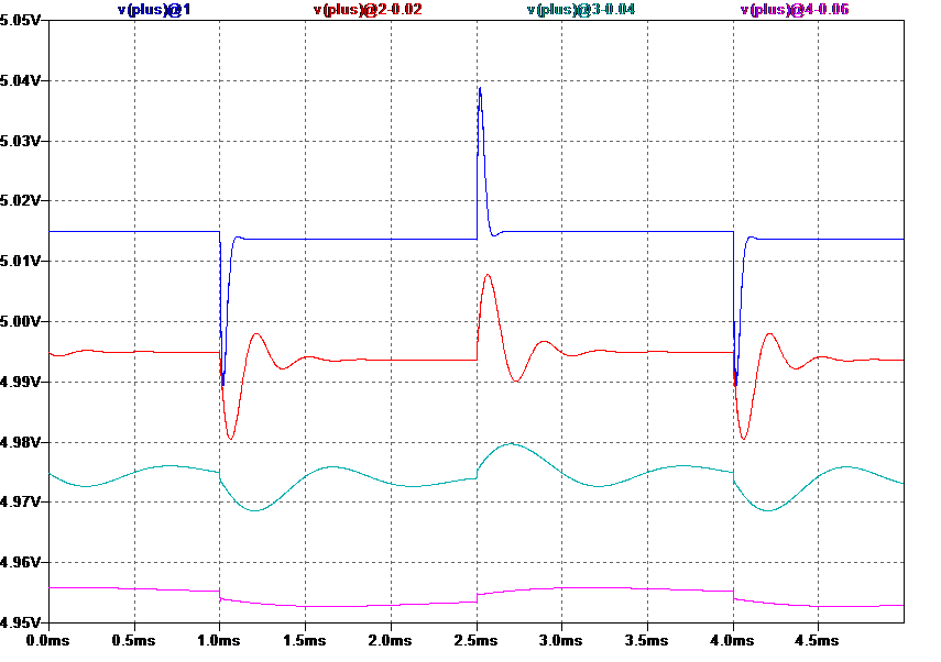
Figure 2.8: the response of figure 2.7 to the 0-10 mA 333 Hz square wave. Talk about ringing!
Still to come: we’ll look at ‘real’ operational amplifiers (well, models of them, anyway) and see what actually happens at their output when their supply pins are waved around. And then we’ll bring those amplifiers and the power supply from this part together. It won’t be pretty! To be continued...
Takeaways from this part:
· Whatever the LDO datasheet says, high-ESR output capacitors give better control of high frequency supply resonances
· The smaller you make the main ceramic decoupling capacitor, the faster and larger will be the ringing that occurs on a load current step – this is a small-signal effect and occurs for any current change, not just large ones.
· If you are designing audio circuits which don’t have impeccable power supply rejection, the LDO regulator impedance bump could cause coloration as it usually occurs within the audio band. Huge output capacitors don’t cure it, in fact they could make it worse. Use that noise bypass connection.
2013 Postscript
Several people expressed surprise at the phase relationship between the waveforms shown on the +ve and –ve supply rails in the many simulation plots in this part. If the load current were flowing directly between the two supply rails, then of course both would shift towards zero. But with the current-steering behaviour of a typical class B amplifier push-pull output stage, the current is either flowing out of the +ve regulator or it’s flowing into the –ve regulator. So a bipolar squarewave load current taken from the amplifier causes an in-phase squarewave voltage shift in both supply rails. The serious consequence of this becomes much more apparent in later instalments.
I also underplayed the importance of having set a static load current on the regulator. The figure legends talk about a load current change of 0 to 10 mA, but in fact it is 20 mA to 30 mA. The output stages of typical regulators don’t behave cleanly at very low currents – in simulation or in the real world. I encountered that very problem the following year with a high frequency filter built using amplifiers with very low quiescent current but delivering quite a lot of current to a capacitor-coupled load. The original local regulator on the board, providing the single supply rail to the filter, showed a noticeable ‘tail’ on the output voltage when it stopped supplying any current because the amplifier was sinking load current, and taking very little current from the supply. This tail got picked up on an inadequately bypassed bias voltage and produced an error that took some tracking down.
I referred several times to the regulator’s” noise bypass capacitor”, and this caused a bit of confusion because there was no schematic in part 2 to remind people what that meant. It’s the additional capacitor that you can fit to some regulators I chose in order to reduce the output noise contribution of the regulator’s internal reference. It does this by reducing the closed-loop bandwidth of the regulator, which in turn pushes its apparent output inductance down. If you’ve got the space and budget, I really recommend using regulators with this capability, whatever you’re doing. Changing to a cheaper regulator has got several USB audio customers into trouble recently. The USB data transfer causes a supply current modulation at 1 kHz, and that can cause a subtle gain modulation in many audio DACs, because their transfer characteristic is proportional to the supply voltage. The 1 kHz ripple on the supply was about 300 microvolts in one case, undetectable on a scope, but sticking out like a sore thumb as -80 dBc modulation products spaced away from the test signal by 1 kHz on each side. So it was very hard to spot when the test signal frequency was 1 kHz (work it out). Don’t use 1 kHz as the default test signal frequency in a USB audio system!