
Yet More On Decoupling, Part 3 – Some gain, some pain

Last time on “Yet More...” we looked at the impedance of a typical regulator and decoupling capacitor combination, and showed what happened when you ‘shock’ it with some dynamic current consumption. Now we’re going to look at whether we should be concerned about the wobbling supply voltage that analog components will experience when connected. We’ll focus on a staple ingredient of the analog designer’s toolbox: the op-amp.
“Bah, Humbug!”, I hear from somewhere in the audience. “Modern precision op-amps are so fantastic that their enormous power supply rejection will extinguish any possible effect that varying supplies could have on a circuit! My dear boy, decoupling capacitors are only there to quell the evil spirits of oscillation, they don’t actually affect the performance of the circuit! Simulate the power supply rail? Haven’t you got anything better to do with that new-fangled slide rule of yours?”
Well, we’ll see. By now, most analog engineers are (or should be) wise to the myth that “op-amps have almost infinite gain and everything is sorted out by the negative feedback loop, whose properties completely dominate the closed-loop performance”. However, despite huge advertised ‘open loop gains’, it is the destiny of any op-amp’s gain curve to trend downwards at roughly 6 dB per octave until at some frequency (the unity-gain frequency, numerically equal to gain bandwidth product in simple cases, though the terms don’t mean the same thing), there’s none left, it’s just unity, or 0 dB. As frequency rises, falling loop gain means a falling amount of feedback to correct errors inside the loop. What’s more, some amplifiers don’t even have very high low frequency open loop gain either. This is particularly true either of very fast amplifiers or very cheap amplifiers.
OK, so we may not have that much loop gain, but why does it matter – surely a competent designer can suppress the sensitivity to supply rail variations just through architecture choices. Not so! Here’s a blunt assertion you may not have seen before: it is not possible to build a conventional op-amp (a pair of differential inputs, two power pins, one single-ended output pin) that is insensitive to voltage variations on one or other of its power pins. The device converts the voltage difference between the signal inputs into a single-ended output – but that output has to be referenced to something other than ground, because the op-amp doesn’t have a ground pin! Depending on the design, the output voltage will be referenced either to one or other supply pin, or to a voltage somewhere along a potential divider between those two pins (think of it as produced by the ratio of output conductances of the current paths in the main gain stage to the two supply pins).
So, you can’t build a precision op-amp that behaves like it had its own private voltage regulators inside to prevent the output voltage from moving when the supplies do. That kind of device would require a ground connection to reference those private regulators to, which our standard pinout does not give us. And indeed this is borne out by the PSRR plots in amplifier data sheets, which usually show curves with the same general shape as the open-loop gain. Figure 3.1 shows the open loop gain of LT’s LT1723 and figure 3.2 shows the PSRR of the amplifier when connected as a unity gain buffer. The curves for rejection from the +ve and –ve supplies deviate at low frequencies but are very similar above 1 MHz.

Figure 3.1: the open-loop gain response of the LT1723 to signals applied at its input pins.
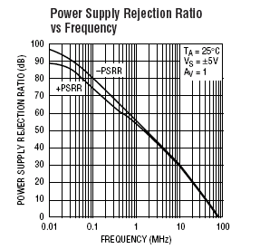
Figure 3.2: the closed-loop gain response of the LT1723 to signals applied at its power pins.
The question of common-mode performance effects on the input stage is a complicating factor and I want to skirt round that for this article. Of course the input stage is attached to the power supplies, and the apparent input voltage at the device can be distorted by the input stage’s reaction to supply variations. But, unlike the power supply rejection problem, this one is amenable to design, layout and processing fixes. Also, the common mode rejection capabilities of current-feedback amplifiers often fall short of good voltage mode op-amps. For clarity of purpose, I’ll use voltage-feedback op-amps in an inverting amplifier configuration as my circuit under test. This means that the input stage only has to reject the (hopefully small) supply variations, and not any applied input signal as well.
Figure 3.3 shows a basic test fixture for measuring the power supply gain (PSG) of a simulation model. The PSG is just the ratio between the small-signal voltage response at the output pin (with respect to ground) to the voltage variation applied to the supply pin (again with respect to ground). The component values depend on whether we’re testing the open-loop (OLPSG) or closed-loop PSG. For the open-loop measurement, we ensure that a good operating point is set by a feedback loop with such a large time constant that it doesn’t allow AC feedback at any frequency we’re simulating over. For the closed-loop test, we just run the amplifier at a gain of ‑1, by editing the capacitor’s value down from very large to very small. Three sweeps are taken here: all the voltage on the +ve rail, all on the –ve, and half on each (i.e. each supply voltage moving, symmetrically with respect to ground).
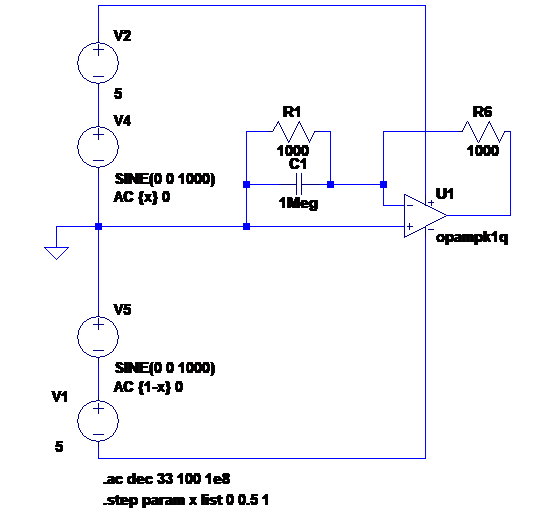
Figure 3.3: the op-amp PSG test fixture, configured with a huge capacitor for open-loop measurement.

Figure 3.4: a simple op-amp macromodel with specific +ve and –ve PSG ratio set by E1.
There are two OLPSG values, one for each supply pin. The observation that the output voltage must be referenced to some voltage at or ‘between’ the two supply voltages has a consequence that I’ll state without proof here: the two values of OLPSG, expressed as a linear factor, must add up to unity at any frequency, regardless of topology. Figure 3.5 shows the OLPSG values for a made-up amplifier model (figure 3.4) designed to have 12 dB better +ve supply rejection than –ve supply rejection, at all frequencies.

Figure 3.5: the OLPSG of the simple amplifier model for just +ve, just –ve and symmetrical cases.
This is a very simple macromodel and has only one internal node, which the output voltage is referred to. Note that this model has no connection to the public ground node in SPICE; this is important, so hold that thought.
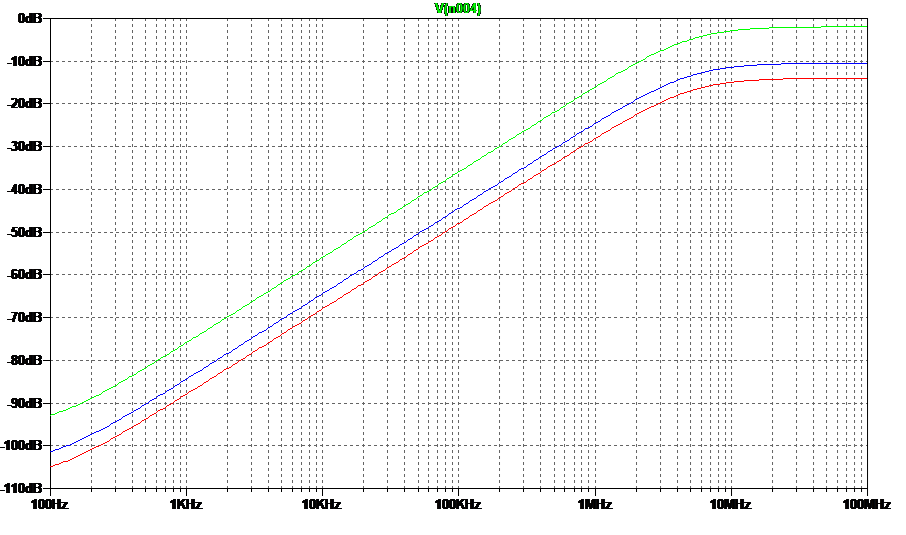
Figure 3.6: the A=‑1 closed loop PSG of the simple amplifier model for the three supply cases.
Without feedback, the OLPSG is a flat line, with the response to unit stimulus on the +ve line (red trace) being 12 dB lower than that for the –ve supply (green trace). The symmetrical case, with half the ripple on each rail, is shown in blue. You can easily calculate that the linear gain values from the red and green traces will sum to unity. This will always be the case, whatever ratio we set in the model for the ratio between +ve and –ve PSG. What is more, if we make the ripple on the supplies move in the same direction on each rail, the open loop output signal equals the supply ripple voltage
When feedback is applied (figure 3.6), we’ll therefore get a result that shouldn’t surprise; at frequencies above the unity gain frequency (set to 10 MHz for this amplifier model) the rejection is the same as in the open-loop case, and the rejection improves by 6 dB for every octave we fall in frequency from that point. Flip this curve around the frequency axis and you get the standard PSRR curve beloved of amplifier suppliers.
Let’s double-check. In figure 3.7 the excitation on the supplies is set to in-phase, rather than symmetrical, and the closed-loop gain is swept from ‑1 to ‑1000. We see that the high frequency gain is always 0 dB (this is with the same amplifier with differing +psrr and –psrr by design and that, as you require more application gain from the device, this power supply gain is available down to lower and lower frequencies.
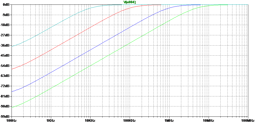
Figure 3.7: the PSG to the amplifier output, both rails in phase, as gain increases from ‑1 to ‑1000.
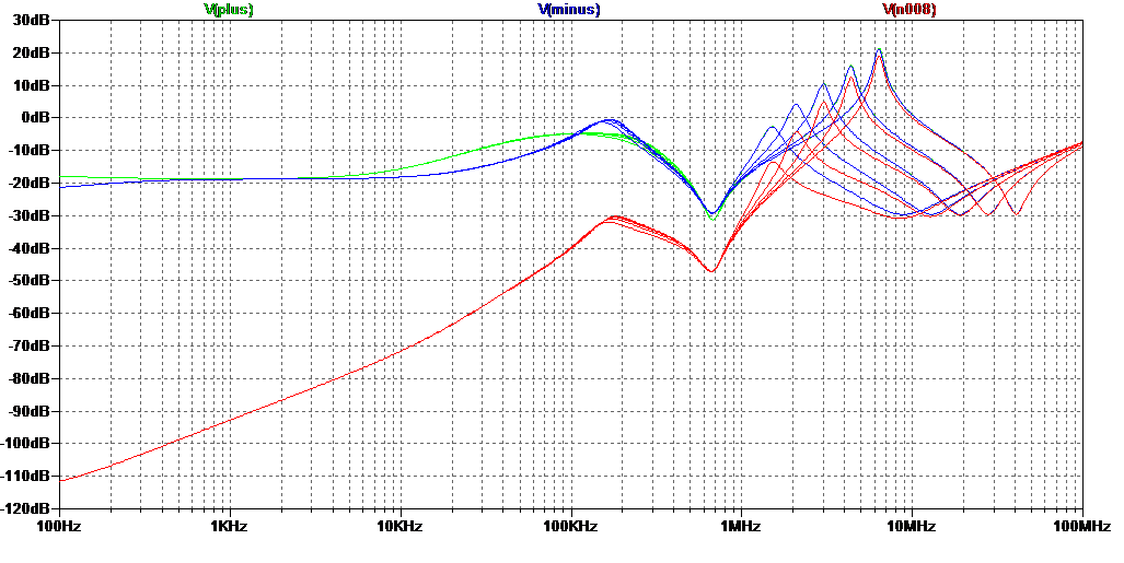
Figure 3.8: Those supply capacitor resonance peaks right there at the amplifier output (red traces).
Want a sneak preview of what’s coming next? Let’s fire up our power supply and actually have a look at the output of this amplifier. Figure 3.8 shows this; the green and blue traces are the familiar regulator responses from way back in part 1. The red traces are the op-amp output, and we shouldn’t be surprised that at frequencies above 10 MHz the op-amp output contains exactly the same signals as the power supplies. Let’s fix the decoupler to 100 nF and sweep the closed-loop gain of the amplifier instead. Figure 3.9 shows the results, figure 3.10 the test fixture. Where has all the supply rejection gone?
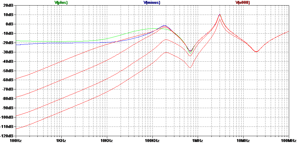
Figure 3.9: as we increase the gain of the amplifier, more of the supply response appears at the output.

Figure 3.10: where we’ve got to so far, fixture-wise.
OK, that’s enough for now, let’s not spoil the surprise of part 4. To be continued...
Takeaways from this part:
· Op-amps must have power supply rejection behaviour that tracks their open-loop gain, if the results on both supply pins are taken into account
· Op-amps do not have a ground pin, and therefore op-amp models should not make a connection to SPICE’s public ground net. This can cause problems that aren’t apparent in simulations where the supply voltages are perfect with respect to ground
2013 Postscript
A few times after this instalment came out I had to walk through the argument, given in the fourth paragraph, that op-amps cannot possibly, ever, under any circumstances, have perfect supply rejection from both power terminals.
The short way of putting it is this: in order to guarantee that a circuit’s output voltage will not vary with respect to ground, when an of its supply voltages is varied with respect to ground, it must know where ground is. And an op-amp doesn’t. If you pick a cat up by all four legs, the nose will follow. Legs = supply pins, nose = output pin. It’s a much less silly analogy than you might think. Obvious, really, so quite why people think cat manufacturers will ever be able to change it by cat design or feedback, I really don’t know…
Then I introduced the acronym PSG, for power supply gain, and some people thought it was a standard term they’d not heard of. It’s not, but I think it should be. As I commented later, it’s really just the inverse of the power supply rejection ratio, but it’s much more useful for grasping the in-circuit impact of wiggling those supply pins about – especially when some feedback is applied. I’m certainly not the first person to write about the need to think of the supply pins as inputs. If I made a small contribution, it was to point out that there’s no escape from their input-ness and it always needs to be taken into account.
I probably labored these points a little, allowing the dramatic tension to sag a little in the middle, as it does in some thrillers. But the important stuff does begin to come into focus in this episode. Because no amplifier can completely reject the variation of the voltage on its supply pins, regardless of the topology employed, this variation will always be visible on the output terminal in some form. And in the worst-case, but highly likely, scenario, introduced in the previous episode, of an in-phase variation caused by the very load current the amplifier is sourcing and sinking, the result is utterly predictable and, again, topology- and manufacturer-invariant.
Supply voltage variations will make an op-amp’s output voltage move. Any data sheet or app note that implies that it won’t, is wrong. So there.